Power of Power Integrity Analysis in High-Speed Digital Designs

The Emergence of Power Integrity Analysis
As the speed of the data signal increases, many reasons including power supply noise lead to the degradation of the high-speed signals. In low power high-speed digital interfaces, it is crucial to characterize the whole system power supply in order to minimize power supply noise in the system. High-speed design failures show up as failures at higher operating frequency, data error rates, cross talk errors, and EMI errors. Currently, PI engineers do PI analysis of power system to ensure proper and reliable operation using Electronic Design Automation tools (EDA) before the actual fabrication of board. This reduces board failure chances significantly and also cuts production time.
SI and PI are two distinct but related realms of analysis concerned with the proper operation of digital circuits. In SI, the main concern is to make sure that transmitted 1s looks like 1s at the receiver (and same for the 0s). In PI, the main concern is to ensure that the drivers and receivers are provided with adequate current to send and receive 1s and 0s. SI and PI analyzes concerned with the proper analog operation of digital circuits, therefore; care must be taken at the design stage itself to ensure that the design is in accordance with high-speed design rules.
Power Delivery System
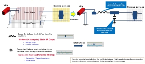
In High-speed digital (HSD) boards there are many power planes. The main focus of Power Integrity Analysis is to find out the PDN complex impedance Z(f) of the complete power system that defines, together with chip current waveform, the voltage variations on-chip power rails. The PDN will act not only as a means of delivering current to ICs, but also as a return current path for signals. A great deal of the crossovers between signals and PI occurs at vias, and for a single-ended signal passing through a via, it is the PDN that acts as the return current path for that signal. To achieve good power integrity, we want the PDN to have the lowest impedance possible. At dc, that means having as low a resistance as possible in the plane shapes. At ac, that means minimizing the impedance between power and ground. That impedance will vary based on where on the board you are—where you place capacitors, how they are mounted, and what type and value of capacitor you use.
In fact, finding that impedance at different locations on the board is often the biggest part of the task in power integrity analysis. Often called decoupling analysis, the goal of this exercise is to find the impedance between power and ground at different locations on the board, usually at the power pins.
In fact, finding that impedance at different locations on the board is often the biggest part of the task in power integrity analysis. Often called decoupling analysis, the goal of this exercise is to find the impedance between power and ground at different locations on the board, usually at the power pins.
This article will highlight the role of simulation in the design of PCB power delivery network (PDN) systems, including the voltage regulator module (VRM), decoupling capacitors (decap), and the spreading parasitic of the power/ground plane. The PDN analysis will focus on both the static case (DC or voltage or IR-Drop) and AC analysis in the frequency domain, with the main focus on PDN impedance. In addition to the AC analysis, I will also demonstrate the decap role to minimize power plane impedance.
Power Integrity (PI) Analysis
In power integrity analysis, the main types of simulations are dc voltage drop analysis, decoupling analysis, and noise analysis. First, dc voltage drop analysis involves the analysis of complex trace and plane shapes on the PCB to determine how much voltage is being lost due to the resistance of the copper. In the PI analysis, energy is distributed through transmission planes that make the analysis more complex than basic SI, since energy is moving in x and y directions, as opposed to just one direction down the transmission line.
DC Simulation
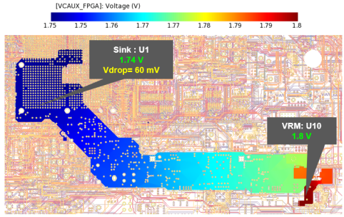
PI-DC analysis computes the voltage, IR drop (voltage drop), current, and power loss density in the power supply nets. Using this analysis, it is identified how much current is drawn by IC and connector pins or stitching vias at DC operating conditions. Due to excessive voltage drop, the power supply voltage at the IC might fall below the recommended minimum voltage. This can cause malfunctioning of the IC. Excessive current density in the perforated power supply rails can generate excessive heat, which might lead to board failures due to delamination or fusing. Also, excessive current in the stitching vias can lead to failures losing connection. Any number of power supply nets with source and sink models can be simulated together. The simulated DC IR drop result of 1.8 V VCAUX power plane is shown in Fig. 3. The maximum voltage from VRM to sink (ICs) is 60 mV. Similarly, all PDNs are simulated to get the max voltage drop in power plane.
AC Simulation
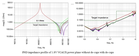
At DC, modeling is relatively simple so that the series resistance of traces, plane shapes, and vias need to be calculated. But, for high frequencies, analyzing the impedance between power and ground at various locations on the PDN requires complex calculations. PI-AC analysis computes the impedance for the IC current loads over a broad frequency range. It helps to identify whether the PDN provides a low impedance path from the VRM to the IC. AC analysis is carried out to find out the PDN impedance seen from the IC. The VRMs provides 0.9 V to 5 V, the IC pulls 0.1 to 6 A, and a 5% tolerance on the supply voltage is allowed up to around 300 MHz. The result and target impedance is shown for VCAUX power plane in Fig. 4. Target impedance 0.1 Ω is the green line. At higher frequency, the target impedance specification is more relaxed and rises with frequency. Excessive impedance in a certain frequency range can generate excessive voltage noise, which is also called dynamic IR drop, when the IC power supply pins draw large amounts of transient current required for I/O or core logic switching at rates that fall into that frequency range.


Comments
Post a Comment